Intel's New EUV Tech A Gamechanger: Can Give It Edge Over Qualcomm, MediaTek

KEY POINTS
- Deep UV lasers have been traditionally used in manufacturing chipsets
- EUV technology can help manufacturers create more efficient chipsets
- It is a more viable alternative to deep UV for making 4-5nm chipset components
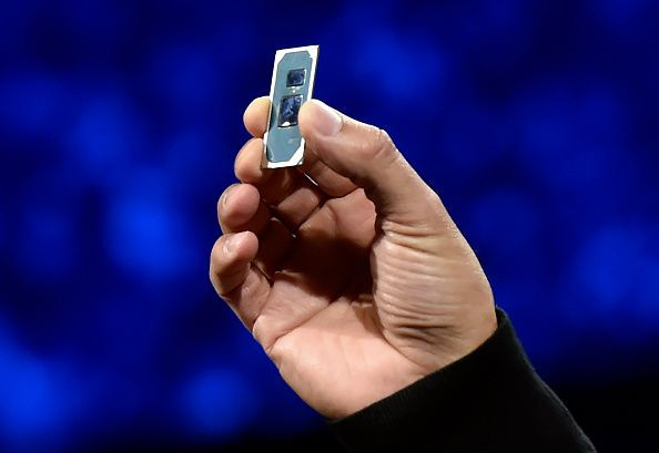
Intel has been working on perfecting Extreme Ultraviolet (EUV) lithography for a long time. The technology may provide the company an edge in smartphone chipsets, to compete with the likes of Qualcomm and MediaTek.
The evolution of chipsets from the 10nm process to the 7nm process has thrown up unique challenges. Currently, the parts of the transistors on the chipset are as small as 7 nanometers, while deep ultraviolet light laser used to create them has a wavelength of 193nm. This makes getting the atom-scale accuracy to create efficient processors difficult.
Manufacturers were able to achieve minute designs in the past by multiple patterning – they exposed metal wafer base of the chipset twice or thrice to achieve a set pattern. Complex chipsets require as many as 20 such layers, which makes it a 1,000-step process. This process was labor-intensive and created room for errors.
The EUV process created by Intel may be a solution for creating more efficient and quick-performing processors. EUV projects a chip blueprint on silicon using a 13.5 nm laser – an incredibly small wavelength, compared to deep UV. This helps manufacturers make chips at a minute scale that wasn’t efficiently possible with the previous technology. It can lay down a pattern using a single exposure, at a much better resolution.
But EUV comes with its own challenges -- it is a very difficult light to control. The downtime of EUV machines has also been a bottleneck in its full adoption in the chipset manufacturing process. But Intel is ramping up the process for high-volume manufacturing and things are expected to pick up this year.
One of the factors that will be necessary for EUV adoption is cost. Deep UV plants cost billions of dollars to set up. Converting deep UV plants to EUV is expected to only add to this cost.
While the production of components such as displays has changed dynamically over the years, chipset manufacturers have persisted with deep UV plants, despite the components becoming increasingly smaller -- from 10nm in older chipsets to 7nm in the current processors. In fact, future processors are expected to have even smaller components of 4nm-5nm size.
The reason behind this is the cost of replacing Deep UV with EUV lasers. Companies such as Qualcomm and MediaTek are deeply invested in such machines and are expected to continue with them despite EUV becoming a viable alternative.
The advantage of EUV, seemingly, is that it will be a quicker and more accurate process and combined with a large production line, could result in a faster output of microchips – manufacturers will essentially be able to produce much more efficient chipsets at a quicker turnaround time.
The key to EUV’s success and its becoming an eventual replacement for the current process will be output. EUV does give Intel a leg-up from the competition, especially since it is not as invested as Qualcomm and others in Deep UV.
The company has set up facilities In Oregon, Israel, and Ireland to start production of EUV-based chipsets and is expected to start manufacturing them later this year.
It will be interesting to see how the future of smartphone processing tech pans out and how its new tech will help Intel position itself in that landscape.

© Copyright IBTimes 2024. All rights reserved.


